
Copyright@2016 chegg.com
Solution Authoring
Guidelines
Version 9.4
September 2016

2
Copyright@2016 chegg.com
Subject-specific Guidelines - Electrical Engineering
Table of Contents
EE1.Content: ...................................................................................................... 3
A. Text/explanation: .......................................................................................................... 3
B. Equations: ..................................................................................................................... 3
C. Diagrams: ...................................................................................................................... 3
D. Tables: ........................................................................................................................... 4
EE2.Technology: ................................................................................................ 6
A. MATLAB: ..................................................................................................................... 6
B. OrCAD/PSpice: .............................................................................................................. 7
C. Multisim: ....................................................................................................................... 8
List of changes made over Version 9.1
(A) Graphs in EE1 has been removed.
(B) Point 1 in A. Text/Explanation has been removed ……………………………………….…………….Page no. 3
(C) Point 2 in C. Diagrams has been removed and diagram added to the point 3…………….Page no. 3
(D) D. Graphs have been removed from EE1. Content………………………………………………….….Page no. 3
(E) More clarity on tables has been provided in D. Tables……………………………………………….Page no. 4
(F) Replaced the section EE2. B with new information…………………………………………….….….Page no. 7
List of changes made over Version 9.3
(1). Modified example part under A. Text/Explanation in EE1. Content…………………………….3
(2). Modified the first sentence in example of second point under B. Equations……………………..3
(3). Added fourth and fifth points under C. Diagrams………………………………………………..4
(4). Third bullet point under D. Tables……………………………………………………………….4
(5). Note added at the end of D. Tables………………………………………………………………5

3
Copyright@2016 chegg.com
EE1. Content:
A. Text/explanation:
1. The conclusion statement should reflect the question. Any inferences from the
solution can be mentioned in the conclusion section.
Example: Thus, the minimum power rating of each resistor,
P
is
8.51 kW
.
B. Equations:
1. The degree symbol should be used while describing the temperature in case of
centigrade, Fahrenheit and Rankine
C, F, RT T T
. The degree symbol should
not be used for Kelvin—instead, use
KT
.
2. In some textbooks, equations are in Math style and in others they are in Text style.
Math and Text are style options available in MathType /Microsoft Equation 3.0.
Always follow the style of the textbook.
Math style: Text style:
2
12
ref CC
R
vV
RR
2
ref CC
12
R
vV
RR
Mathematical equations for Fourier and Laplace Transforms should be standard.
Example: The input signal is
t
x t e u t
.
The Fourier Transform of
xt
,
1
X
j
.
The Laplace Transform of
xt
,
1
Xs
s
.
3. Brackets “[]” should be used outside the parentheses “()”.
Example:
2
2
2 3 2V x x
C. Diagrams:
1. If the solution should start with the given circuit diagram in the problem, ensure
that there is some modification or additional label that is relevant.
2. Figures and graphs should be numbered sequentially and properly labeled.

4
Copyright@2016 chegg.com
3. In phasor diagrams, all representations (arrows, directions, colors and notation)
should be differentiable.
4. Circuits that do not require software simulation should be drawn using Draw Plus /
Corel Draw. Do not use EE software (like pspice/Multisim/etc.) to draw such circuits.
5. Do not use MS word tools to draw circuit diagrams or K-Maps.
D. Tables:
Titles should be brief and informative. Tables should be numbered at the top
followed by the title.
Include explanatory notes below the table.
In truth tables and Karnaugh maps, all cells should have their entries center-aligned.
Provide MathType or image type tables instead of using word table. The titles should
be in bold.

5
Copyright@2016 chegg.com
In digital circuits, mappings should be distinguishable with different
colors.
Note: Give the title for figure/table, only if the figure/table is referenced in the solution.
6
Copyright@2016 chegg.com
EE2. Technology:
A. MATLAB:
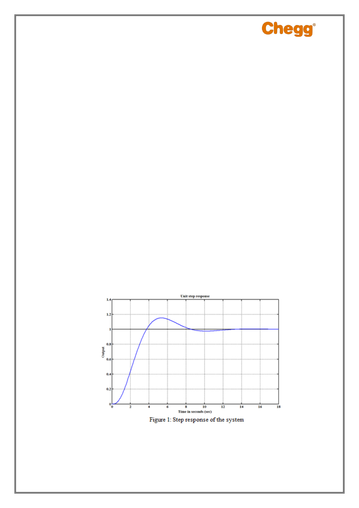
Adhere to the procedures used in the textbook that you are working out of.
If any code is used in the solution for solving complex equations or to get graphical
representations, related code should be provided within the solution.
Example: MATLAB code for plotting step response of a given function
numerator = [0 0 0 1.268];
denominator = [1 3 2.2536 1.268];
step (numerator, denominator)
grid
title ('Unit step response')
xlabel ('Time in seconds')
ylabel ('Output')
Note: Code should be in Courier New font.
The graph line/curve should have suitable width. Font Style of Text/Numbers in the plot
should be Times New Roman.
7
Copyright@2016 chegg.com
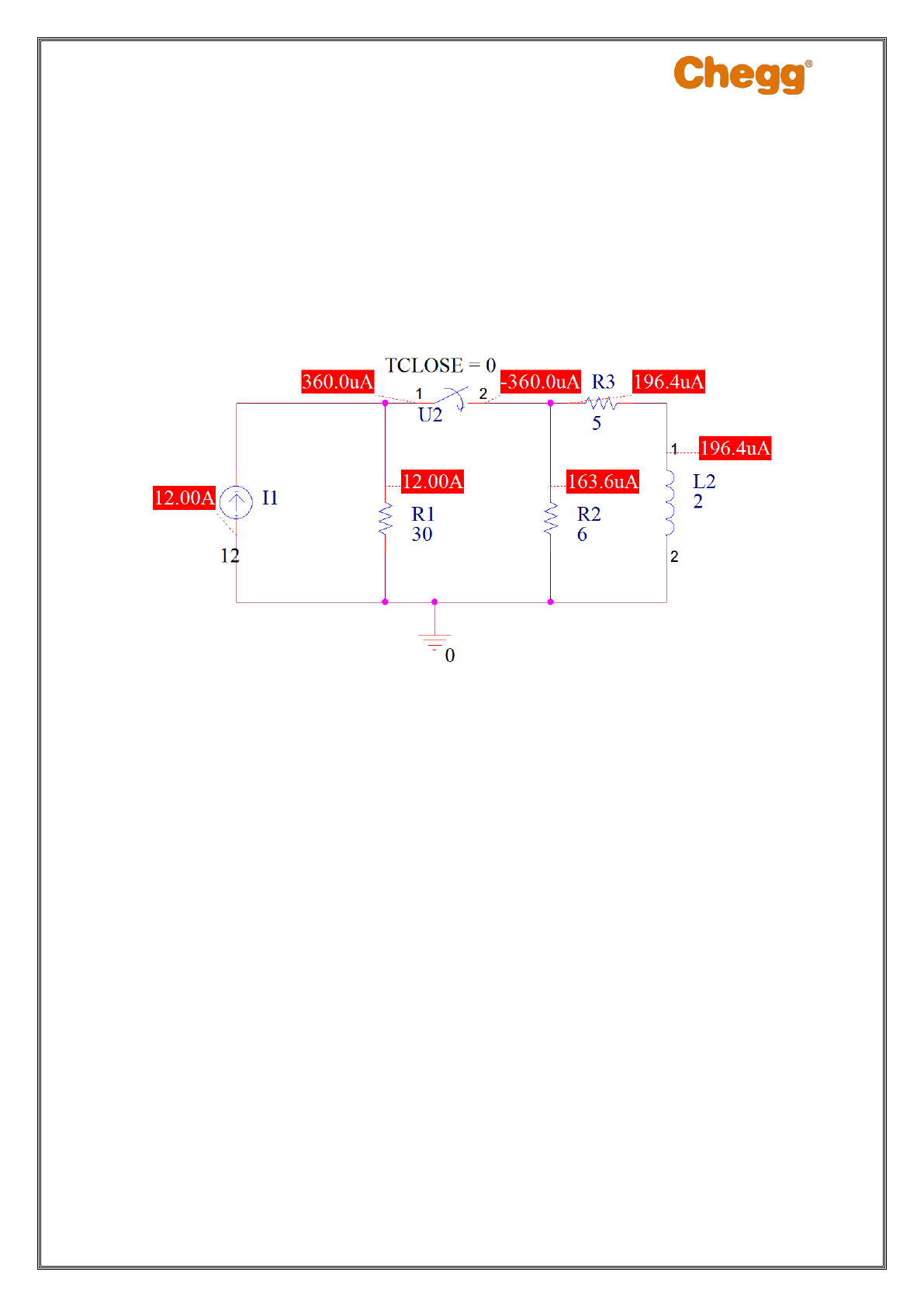
B. OrCAD/PSpice:
Adhere to the procedures used in the textbook.
Use specifications given in the text book for OrCAD based solutions
Symbols used in the simulator should have proper size
Wires should have suitable width
Connectors should be easily differentiable
Text size should be appropriate
Font Type should be Times New Roman and Font size should be 12 (Double Click
on the respective text to change the font type)
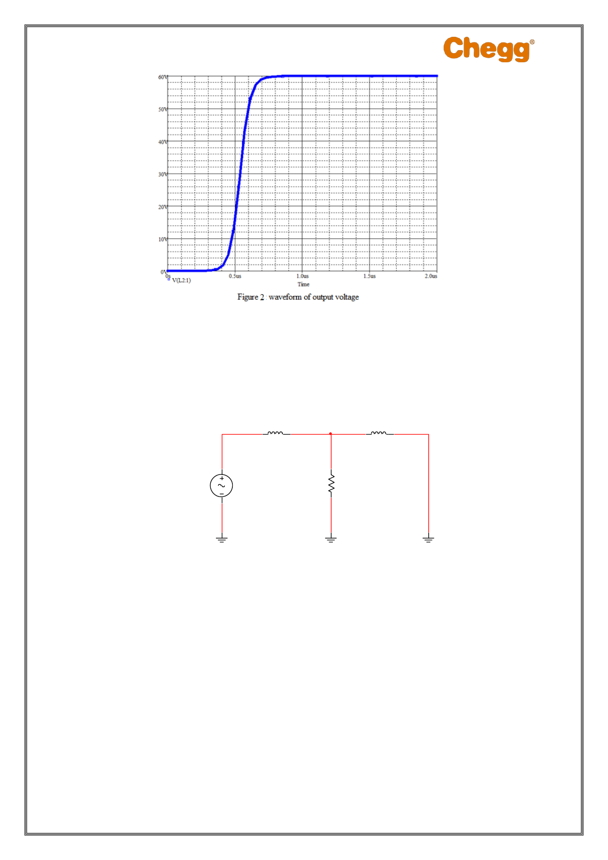
Follow the steps mentioned below to edit the properties of output waveforms:
Right click on the line and select properties. Increase the width and change color to
blue
Go to Page Setup from File menu and set font type to Times New Roman and font
size to 12
Remove Header and Footers and check No Border in the Page Setup
Use PRINT PREVIEW to get the image. Use Print Screen to copy the image into
Paint. Do the necessary modifications in Paint and then copy the image into the word
document.
The waveform generated should be as shown below:
8
Copyright@2016 chegg.com
Simulated soft files of the circuit should be provided along with the original solution.
C. Multisim:
Adhere to the procedures used in the textbook that you are working on.
The schematic diagram should be as per the circuit given in the question.
Follow the meter settings as per the analysis, either ac or dc.
VS
10 Vrms
1.5kHz
0Deg
L1
10mH
IC=0A
L2
10mH
IC=0A
R1
820Ω

9
Copyright@2016 chegg.com
Back

10
Copyright@2016 chegg.com
Example solutions - Electrical Engineering
List of changes made over Version 9.1
MCQ solution modified as per MCQ guidelines in EE example 1……………………Page no. 11
List of changes made over Version 9.2
Existing solution replaced with new solution in EE example 1-MCQ ………………Page no. 11
Fill in the blank type solution added in EE example 7…………………..………………….Page no.32
True or False type solution added in EE example 8….…………………..………………….Page no.33
Very Short Answer type solution added in EE example 9……………..………………….Page no.34
List of changes made over Version 9.3
Tab spaces removed for all equations

11
Copyright@2016 chegg.com
EE Example 1: Multiple-choice type
Question
When the total charge in a capacitor is doubled, the energy stored:
(a) Remains the same (b) is halved (c) is doubled (d) is quadrupled
Solution
Write the formula for energy stored in a capacitor in terms of charge.
2
2
1
2
1
2
w Cv
Cv
C
Substitute q for
Cv
2
2
q
w
C
Here,
q is the charge stored in the capacitor and C is the capacitance of the capacitor
The total charge in the capacitor is doubled and the capacitance of the capacitor remains
unchanged. The new stored energy is,
2
1
1
2
q
w
C
Substitute
2q
for
1
q
in the equation for stored energy in the capacitor.
2
1
2
2
2
4
2
4
q
w
C
q
C
w
Thus, the energy stored in the capacitor does not remain the same. It is not halved or doubled.
Hence, the options (a), (b) and (c) are wrong.
When the charge is doubled, the energy stored in the capacitor becomes 4 times that of the
original energy, that is, the energy stored is quadrupled.
Hence, the correct option is
d
.
12
Copyright@2016 chegg.com
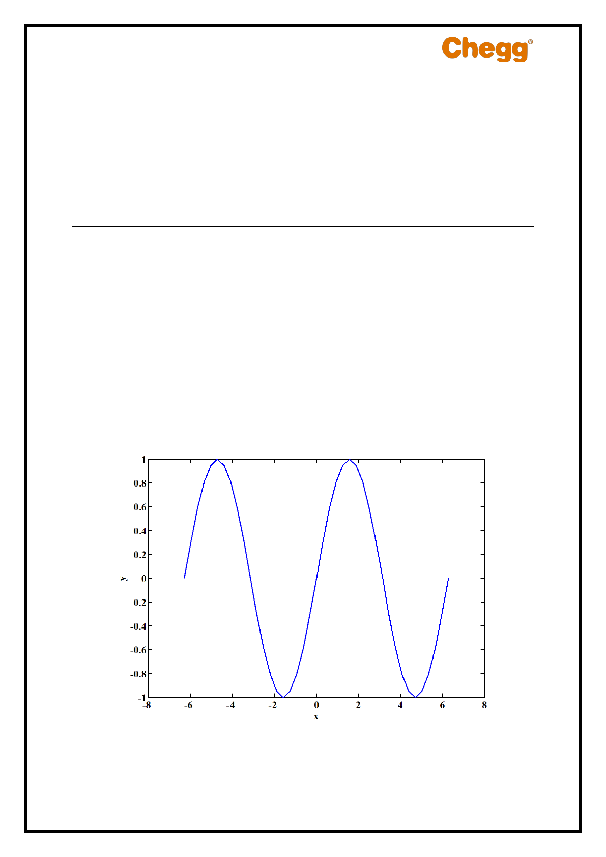
EE Example 2.1: Software type
Question:
Create a plot of the function,
sinyx
for
x
from
2
to
2
(a) Assign a handle to axes created in the main program, and then change background
color to blue.
(b) Assign a handle to axes created in the main program and then change the
x axis
scale to
log
.
Solution:
Create a plot of the following function:
sinyx
for
x
from
2
to
2
Enter the following code in MATLAB to plot the function:
x=-2*pi:pi/10:2*pi;
y=sin(x);
h=plot(x,y);
xlabel x
ylabel y
The following is the MATLAB output:
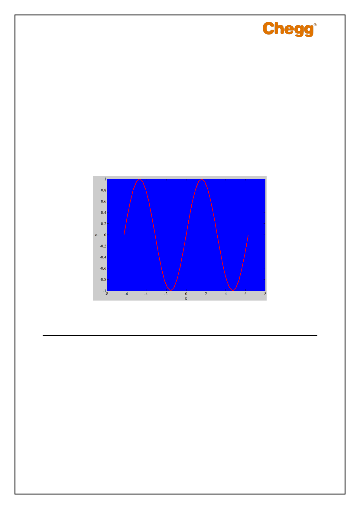
Figure 1
Thus, the plot of the sine function is created.
13
Copyright@2016 chegg.com
(a)
Enter the following code in MATLAB to assign a handle to axes created in the main
program, and then change background color to blue:
x=-2*pi:pi/10:2*pi;
y=sin(x);
plot(x,y,'r');
xlabel x
ylabel y
h=gca;
get(gcf)
set(h,'color',[0,0,1])
The following is the MATLAB output:
Figure 2
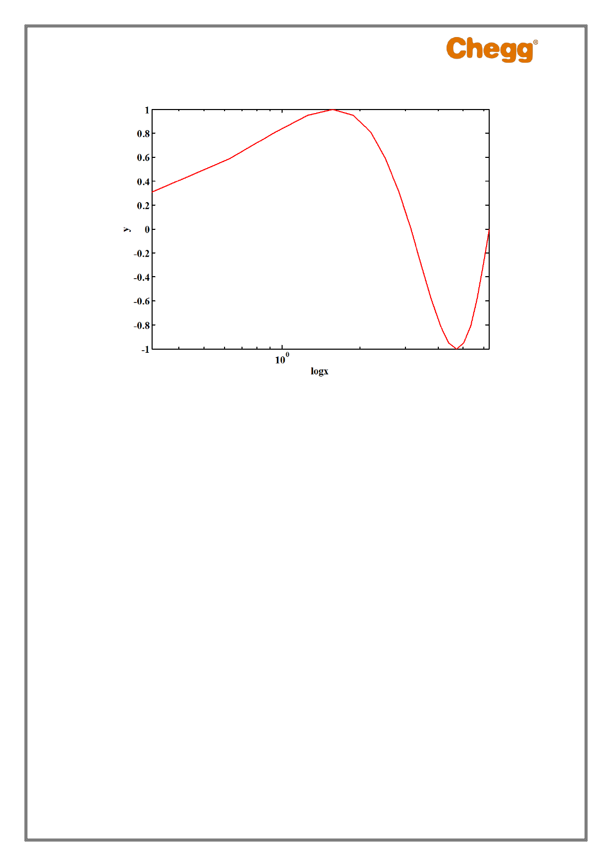
(b)
Enter the following code in MATLAB program to assign a handle to axes created in the main
program, and then change the x-axis scale to log:
x=-2*pi:pi/10:2*pi;
y=sin(x);
plot(x,y,'r');
xlabel logx
ylabel y
h=gca;
get(h)
set(h,'xscale','log')
14
Copyright@2016 chegg.com
The following is the MATLAB output:
Thus, the x-axis scale is changed to log.

15
Copyright@2016 chegg.com
EE Example 2.2: Software type
Note: Provide software/coding related outputs even though it is not asked in the
question.
Question:
Write a MATLAB program that determines whether or not a given integer is a prime number
(Here, it is asked only to write the code)
Solution:
>> x=input('Enter the number to be tested');
>> for i = 2:x/2
r=rem(x,i);%calculates the remainder when x is divided by i
if r==0
disp('number is not prime')
break
end
end % end loop
if r~=0
disp('number is prime')
end
Execute the code by giving a value to x at the command window.
Enter the number to be tested 79
number is prime
Enter the number to be tested 20
number is not prime
16
Copyright@2016 chegg.com
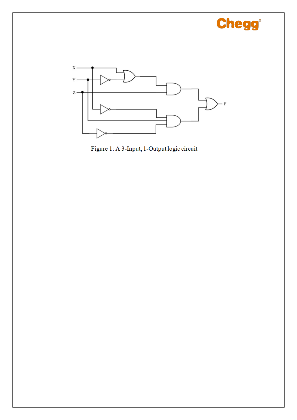
Question:
Write a structural Verilog module for the logic circuit in Figure 1.
Solution:
Refer Figure 1 for the 3-Input, 1-Output logic circuit.
From the figure, the structural Verilog module for 3-Input, 1-Output logic circuit is as
follows:
module Inp3_out1 ( inp1, inp2, inp3, out1);
input inp1,inp2,inp3;
output out1;
wire n1, n2, n3,n4,n5,n6;
not U1 (n1, inp1);
not U2( n2, inp2);
not U3( n3, inp3);
or U4( n4, inp1, n2);
and U5( n5, n4, inp3);
and U6( n6, n1, inp2, n3);
or U7( out1, n5,n6);
endmodule

17
Copyright@2016 chegg.com
The following is the test bench code:
module test_ Inp3_out1;
// Inputs
reg inp1;
reg inp2;
reg inp3;
// Outputs
wire out1;
// Instantiate the Unit Under Test (UUT)
Inp3_out1 uut (
.inp1(inp1),
.inp2(inp2),
.inp3(inp3),
.out1(out1)
);
initial begin
// Initialize Inputs
inp1 = 0;
inp2 = 0;
inp3 = 0;
// Wait 100 ns for global reset to finish
#100;
inp1 = 0;
inp2 = 0;
inp3 = 1;
#100;
inp1 = 0;
inp2 = 1;
inp3 = 0;
#100;
inp1 = 0;
inp2 = 1;
inp3 = 1;
#100;
inp1 = 1;
inp2 = 0;
inp3 = 0;
#100;
inp1 = 1;
inp2 = 0;
inp3 = 1;

18
Copyright@2016 chegg.com
#100;
inp1 = 1;
inp2 = 1;
inp3 = 0;
#100;
inp1 = 1;
inp2 = 1;
inp3 = 1;
end
endmodule
The following is the output of the 3-Input, 1-Output logic circuit:
19
Copyright@2016 chegg.com
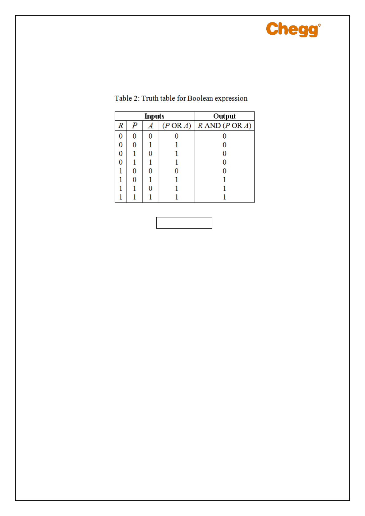
EE Example 3: Tabular type
Question:
A student is allowed to take a course
1C
if he or she pays the registration fee
1R
and
either has the prerequisites
1P
or has the instructor’s approval
1A
.
(a) Give a truth table for C as a function of R, P, and A.
(b) Write a Boolean expression for C.
Solution:
(a)
There are three independent variables namely R, P, A, and one dependent variable C. Thus,
the number of bits
is 3n
and there are
3
28
states.
A student is allowed to take a course
1C
if and only if the following conditions hold:
He or she pays the registration fee
1R
and has the instructor’s approval
1A
He or she pays the registration fee
1R
and has the prerequisites
1P
He or she pays the registration fee
1R
, has prerequisites
1P
, and the
instructor’s approval
1A
The other five combinations forbid a student from taking the course
0C
.
The following is the truth table showing the outputs for all the possible case:
Table 1: Truth table for C
Inputs
Output
R
P
A
C
0
0
0
0
1
1
1
1
0
0
1
1
0
0
1
1
0
1
0
1
0
1
0
1
0
0
0
0
0
1
1
1
20
Copyright@2016 chegg.com
(b)
To compute the truth table for a student who is allowed to take a course
1C
, find the
relations (P OR A) and [
R
AND (P OR A)] to cover all the possibilities.
Thus, the Boolean expression for C is
AND OR R P A
.
21
Copyright@2016 chegg.com
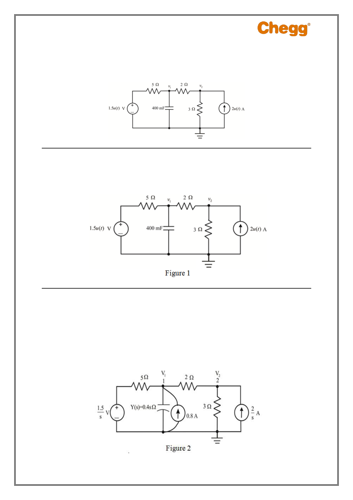
EE Example 4: Calculation Based
Question:
Calculate the power dissipated in the
3
resistor of Figure 1, if
1
0 2Vv
.
Solution:
Consider the following circuit:
The value of
1
0 is 2 Vv
.
Determine the current through the capacitor.
I s sV s (0)
sV s (0)
Cv
C Cv
The s-domain equivalent circuit is shown in Figure 2.

22
Copyright@2016 chegg.com
Apply nodal analysis at node 1.
1
12
1
1.5
(s)
(s) (s)
s
0.4s (s) 0.8 0
52
v
vv
v
12
7 3s
0.4s (s) 0.5 (s) 0.8
10 10
vv
…… (1)
Similarly apply nodal analysis at node 2.
2 1 2
(s) (s) (s) 2
2 3 s
v v v
12
(s) 5 (s)
2
2 6 s
vv
…… (2)
Apply Cramer’s rule to solve equations (1) and (2) and determine the voltages.
2
7 4s 3 8s
10 10s
12
2s
(s)
7 4s 1
10 2
15
26
7 4s 2 3 8s 1
+
10 s 10s 2
7 4s 5 1 1
10 6 2 2
v
2
31 24s
20s
(s)
s1
3
93 72s
20s s 1
v
2
72 93
s
20 72
(s)
s s 1
v
…… (3)
Apply partial fractions to the equation (3).
2
1.291 0.291
(s) 3.6
s s 1
v
Determine the power dissipated in the
3
resistor.

23
Copyright@2016 chegg.com
2
2
2
2
2
(s)
s
3
1 1.291 0.291
3.6
3 s s 1
1.66 0.084 0.751
4.32
s s s 1
s1
v
p
2
2
1.66 0.084 1 1
4.32 0.751
s s s 1
s1
…… (4)
Recall the following inverse Laplace transforms:
1
1
2
1
2
1
1
s
1
s
1
s+1
t
L
Lt
L te
Apply inverse Laplace transform to equation (4).
1
s ( )L p p t
Thus,
( ) 4.32 1.66 0.084 0.751 1
tt
p t t te e u t
Therefore, the power dissipated in the 3
resistor is,
4.32 1.66 0.084 0.751 1 W
tt
t te e u t
24
Copyright@2016 chegg.com
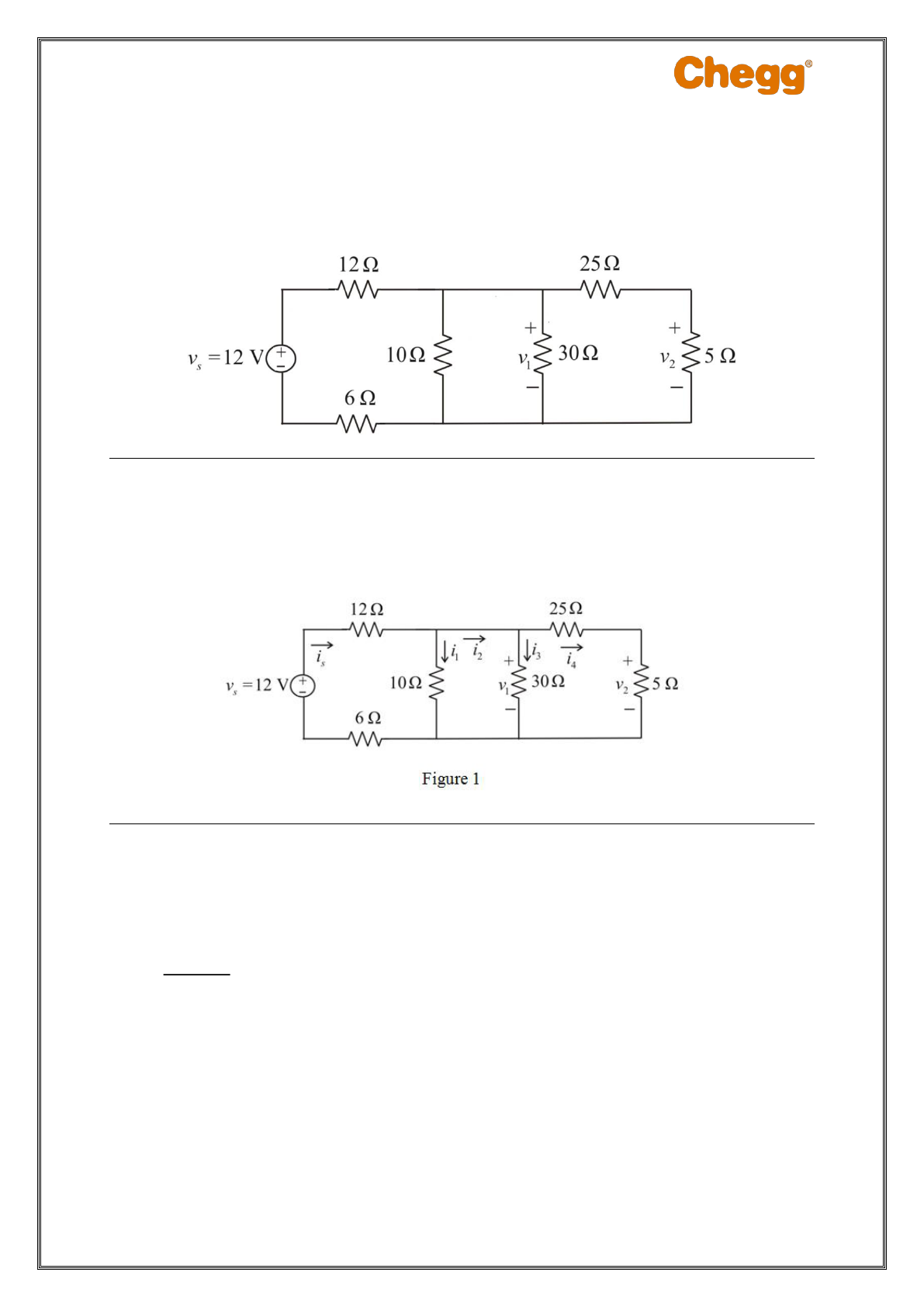
EE Example 5: Diagrammatic
Question:
Find the voltages
1
v
and
2
v
in the following circuit:
Solution:
In the following figure, the resistances
10
and
30
are connected in parallel and the
resistances
25
and
5
are connected in series:
Determine the equivalent resistance of the resistances
25
and
5
connected in series.
eq1
25 5
30
R
Determine the equivalent resistance of the resistances
10
and
30
connected in parallel.
eq2
10 30
10 30
7.5
R
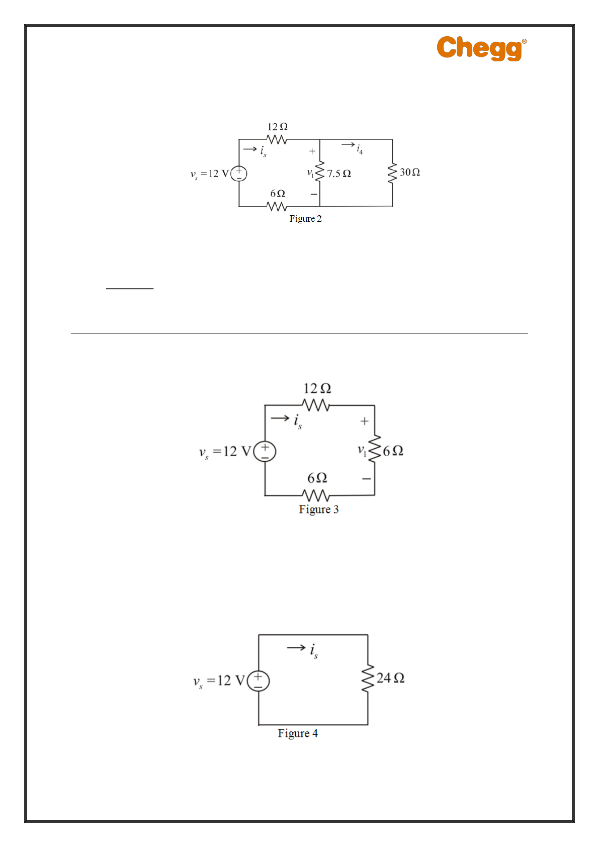
25
Copyright@2016 chegg.com
Redraw the circuit by replacing the series and parallel resistances with their equivalent
resistances.
In figure 2, the resistances
7.5
and
30
are connected in parallel. Determine the
equivalent resistance of the parallel combination.
eq3
7.5 30
7.5 30
6
R
Redraw the circuit with the parallel resistances replaced by their equivalent resistances.
In figure 3, the resistances
12
,
6
, and
6
are connected in series. Determine the
equivalent resistance.
eq4
12 6 6
24
R
Redraw the circuit by replacing the series combination of resistances with their equivalent
resistance.
From figure 4, determine the current
s
i
using Ohm’s law.

26
Copyright@2016 chegg.com
eq4
12
24
0.5 A
s
s
v
i
R
The same current,
0.5 A
flows through the
6
resistance.
From figure 3, use Ohm’s law to determine the voltage
1
v
across the
6
resistance.
1 eq3
0.5 6
3 V
s
v i R
Thus, the voltage
1
v
is
3 V
.
From figure 2, the voltage across the
30
resistance is same as the voltage across the
6
resistance, which is 3 V.
Determine current through the
30
resistance using Ohm’s law.
4
3
30
0.1 A
i
The same current
4
i
flows through the
5
resistance. Determine the voltage
2
v
using
Ohm’s law.
24
5
0.1 5
0.5 V
vi
Thus, the voltage
2
v
is
0.5 V
.
27
Copyright@2016 chegg.com
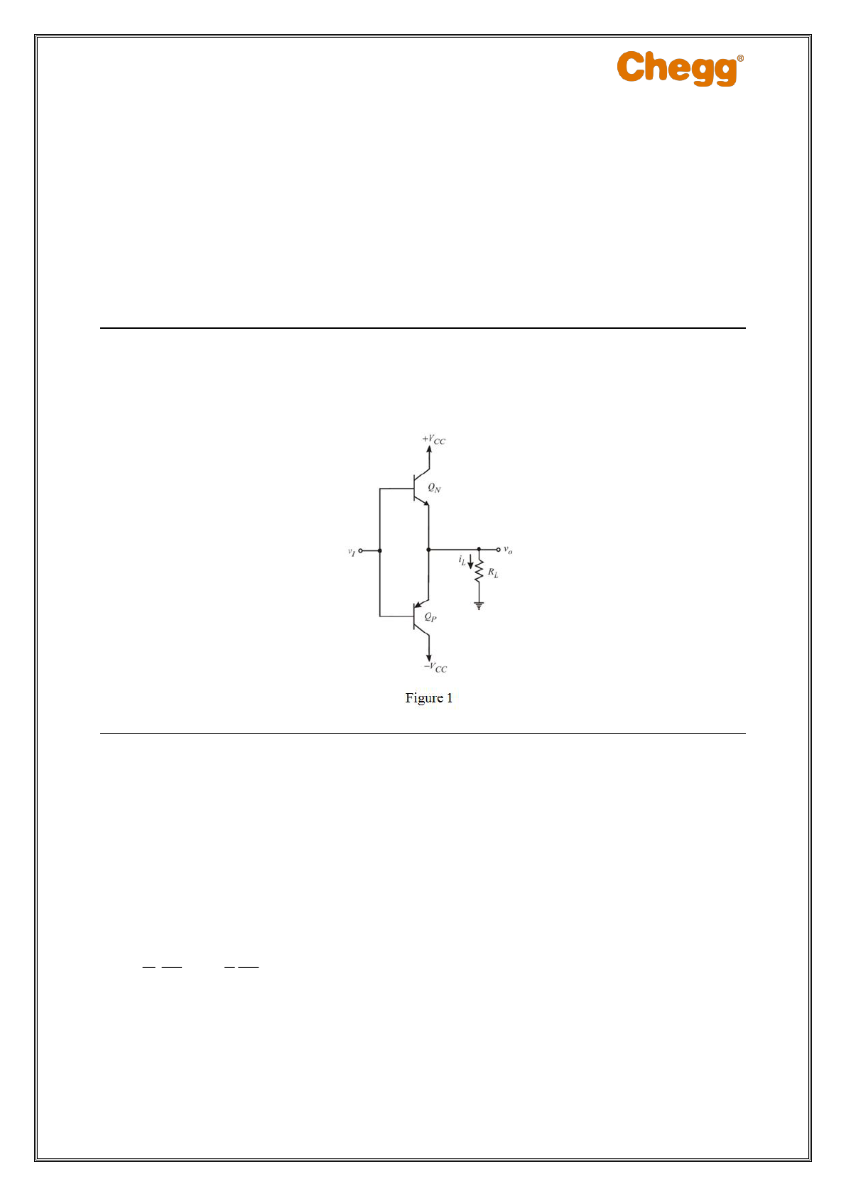
EE Example 6: Lengthy type
Question:
A class B output stage amplifier operates from
5 V
supplies. Assuming relatively ideal
transistors, determine the output voltage for maximum power-conversion efficiency? What is
the smallest value of load resistance that can be tolerated, if each of the output devices is
rated for 1W dissipation, and with a factor of 2 safety margin, and if the operation is always
at full output voltage? What is the smallest load permitted if the operation is allowed at half
the full output voltage? What is the greatest possible output power available in each case?
Solution:
Consider the following class B output stage amplifier:
The supply voltage
is 5V
CC
V
For the maximum power conversion efficiency, the output voltage
ˆ
O
V
is equal to the supply
voltage
CC
V
.
ˆ
5V
O CC
VV
Write the formula for average power dissipated in the class B stage.
2
ˆˆ
21
2
D S L
OO
CC
LL
P P P
VV
V
RR
Here,
D
P
is average power dissipated,
S
P
is supply power, and
L
P
is load power.
28
Copyright@2016 chegg.com
From the symmetry, half of the power
D
P
is dissipated in the transistor
N
Q
and the other half
in the transistor
P
Q
. Thus,
N
Q
and
P
Q
must be capable of safely dissipating power of
1
2
D
P
watts. Since
D
P
depends on
ˆ
O
V
, find the worst case power dissipation
maxD
P
.
Differentiate the average power equation with respect to
ˆ
O
V
.
max
ˆ
2
21
ˆ
2
D
O
P
CC
D
LL
O
V
V
dP
RR
dV
Equate the derivative to zero to get the value of
ˆ
O
V
that result in maximum average power
dissipation.
max
max
max
max
ˆ
2
21
0
2
ˆ
2
21
0
2
ˆ
20
2
ˆ
D
D
D
D
O
P
CC
LL
O
P
CC
LL
CC O
P
CC
O
P
V
V
RR
V
V
RR
VV
V
V
Substitute 5 V for
CC
V
.
max
2
ˆ
2
5
3.183V
D
CC
O
P
V
V
Thus, the output voltage for maximum device dissipation is
3.183V
.

29
Copyright@2016 chegg.com
Derive the formula for efficiency of the amplifier
.
2
2
Load power
Supply power
ˆ
ˆ
2
1
Since, Supply power
2
ˆ
ˆ
2
1
and Load power
2
ˆ
4
L
S
L
S
O
O
s CC
L
L
o
O
CC
L
L
L
O
CC
P
P
P
P
V
V
PV
R
R
V
V
V
P
R
R
V
V
The maximum efficiency is obtained when
ˆ
O
V
is at its maximum, that is,
ˆ
O CC
VV
.
Determine the power conversion efficiency for maximum output voltage.
100%
4
78.54%
Thus, the maximum power conversion efficiency is
78.54%
.
The output device is individually rated for
1W
dissipation, that is,
1 W
D
P
Write the formula for average power dissipated in the class B stage.
2
ˆˆ
21
2
OO
D CC
LL
VV
PV
RR
Rewrite the formula to get the expression for load resistance
L
R
.
2
1 2 1
ˆˆ
2
L O CC O
D
R V V V
P
Substitute
1 W for
D
P
and 5 V for
ˆ
and
O CC
VV
.
2
1 2 1
5 5 5
12
15.916 12.5
3.416
L
R
Thus, the smallest value of load resistance for operating at full output voltage is
3.416
.

30
Copyright@2016 chegg.com
Determine the greatest possible output power available.
2
max
2
1
2
15
2 3.416
25
6.832
3.66 W
CC
L
L
V
P
R
Thus, the greatest possible output power available is
3.66 W
.
For operation at half the full output voltage, the output voltage is half the value of
CC
V
.
ˆ
2
5V
2
2.5V
CC
O
V
V
Recall the formula for efficiency in terms of
ˆ
and
O CC
VV
.
ˆ
4
O
CC
V
V
Determine the power conversion efficiency for operation at half the full output voltage.
2.5
100%
45
39.27%
Thus, the power conversion efficiency for operation at half the full output voltage is
39.27%
.
Write the formula for load resistance
L
R
.
2
1 2 1
ˆˆ
2
L O CC O
D
R V V V
P
Substitute
1W
for
D
P
, 2.5 V for
ˆ
O
V
, and 5 V for
CC
V
.
2
1 2 1
2.5 5 2.5
12
7.9577 3.125
4.833
L
R
Thus, the smallest value of load resistance for operation at half the full output voltage is
4.833
.

31
Copyright@2016 chegg.com
Determine the greatest possible output power available.
2
max
2
1
2
15
2 4.833
25
9.666
2.586W
CC
L
L
V
P
R
Thus, the greatest possible output power for operating at half the full output voltage is
2.586W
.

32
Copyright@2016 chegg.com
EE Example 7: Fill in the blank type
Question
The time constant for an RL circuit with
2 R
and
4 HL
is ____.
Solution
Write the formula for the time constant
for an RL circuit.
L
R
Here,
L is the inductance in the circuit and R is the resistance in the circuit
Substitute
2
for
R
and 4 H for L in the formula for the time constant.
4
2
2 s
L
R
Thus, the time constant for an is RL circuit
2 s
.

33
Copyright@2016 chegg.com
EE Example 8: True or False type
Question
The superposition principle applies to power calculation. True/False.
Solution
Superposition theorem states that in a circuit containing two or more independent sources, the
voltage or current in an element is equal to the algebraic sum of the quantities due to each
independent source acting alone.
The principle of superposition depends on the linearity property.
As the power absorbed by a resistor depends on the square of the voltage or current, it is not a
linear relation. So, the superposition principle cannot be applied to power calculation. Thus,
the statement is not true.
Hence, the statement is
False
.

34
Copyright@2016 chegg.com
EE Example 9: Very Short Answer type
Question
The voltage across a
5 k
resistor is 16 V. Find the current through the resistor.
Solution
Write the formula for current I through the resistor.
V
I
R
Here,
V is the voltage across the resistor and R is the resistance of the resistor
Substitute 16 V for V and
3
5 10
for R in the formula for current I.
3
3
16
5 10
3.2 10 A
3.2 mA
V
I
R
Hence, the current through the resistor is
3.2 mA
.
Back
